Chapter 15 Semiconductor materials
Chapter contents
15.1 Aim
This chapter introduces the reader to semiconductors and semiconducting devices that are important to radiography. This is a very large field, and the chapter concentrates on the barrier layer rectifier, which has made a major impact on radiographic science. After an overview of the development and manufacture of integrated circuits. the chapter concludes with an overview of the used of semiconductor devices in radiography.
15.2 Introduction
The use of semiconductor materials and the associated technology play an increasingly important part in our everyday lives as well as in radiographic science. Today it is possible to produce millions of electronic circuits on a small silicon chip using ultra-large-scale integration (ULSI) techniques. This has enabled the production of microprocessors that are capable of being programmed to perform specific tasks. Such devices are cheap and easy to program. They can perform a wide range of functions and are very reliable. Because of this, microprocessors are found in devices from wristwatches to aircraft flight systems and it is not surprising to learn that they are used in many devices in diagnostic imaging and radiotherapy departments.
However, the microprocessor is a complicated solid-state device and a detailed description of its operation is beyond the scope of this text.
Other, simpler, solid-state devices are widely used in X-ray circuitry and are suitable for inclusion in this chapter after a general description of the properties of semiconductor materials.
15.3 Intrinsic semiconductors
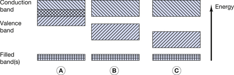
An intrinsic semiconductor is a chemically pure semiconductor, which is also assumed to have perfect regularity of atoms within its crystalline structure or lattice. The concept of semiconducting materials was briefly introduced in Section 7.3.2 where the properties of conductors, insulators and semiconductors were compared in terms of the energy band model for the orbiting electrons. This was illustrated in Figure 7.2 and this diagram is reproduced here as Figure 15.1 (below). As shown in Figure 15.1B, one of the characteristics of semiconductors is that there is a small energy gap (up to a few eV) between the top of the valence band and the bottom of the conduction band. At very low temperatures, all the outer electrons have energies near the bottom of the valence band, and no electrons are able to take part in electrical conduction, as there are no free electrons in the conduction band. As mentioned in Chapter 7, increasing the temperature of a semiconductor increases its conductivity. At normal room temperatures, many electrons are able to gain sufficient energy (because of the increased kinetic energy of the atoms) to jump up to the conduction band and so take part in electrical conduction.
15.3.1 Positive holes
Associated with each electron which is able to jump up to the conduction band is a ‘vacancy’ in the valence band, referred to as a positive hole or just hole. This hole may be filled by an electron from the valence band of a neighbouring atom, but in doing so the electron leaves a hole in the valence band of that atom. In this way, a hole may appear to move around the crystal lattice of a semiconductor (behaving like a positive charge) until eventually an electron drops down from the conduction band to fill the hole and remove it from the valence band. This process is referred to as recombination. At any one moment in time, all three of the above processes are occurring:
1. Electrons are being excited into the conduction band creating holes in the valence band.
2. There is movement of electrons in the conduction band and holes in the valence band.
3. There is a recombination of electrons in the conduction band with holes in the valence band.
The overall conductivity of such an intrinsic semiconductor is the sum of the effects of the movements of the electrons in the conduction band and the holes in the valence band.
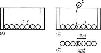
Consider the situation depicted in part A of the diagram below, where there is a row of ball bearings at the base of a box, with no available space between them for sideways movement to take place. If we now lift ball bearing C onto the lid of the box, it is possible for ball bearing D to move to the left to fill the space once occupied by C. In doing so, D has now created a space to its right, i.e. the hole may be considered as moving in the opposite direction to the ball.
Now consider the above situation as it refers to the valence and conduction bands of a semiconductor. No net movement is initially possible in the valence band because it is full of electrons. When an electron is raised to the conduction band, movement within the valence band is possible. Thus, if an electron moves from right to left within the band, it leaves a hole in its starting position, i.e. the hole appears to move from left to right. If an electron is removed from the valence band of an atom, then the atom is positively charged since the protons in the nucleus now outnumber the orbiting electrons; the hole is referred to as a positive hole. If a semiconductor is passing a current such that the electron flow in the conduction band is from left to right, there will also be an effective flow of positive charge associated with the movement of positive holes in the valence band in the opposite direction.
15.3.2 Silicon
Silicon is currently the most widely used general semiconductor material. It has an atomic number of 14 and has 14 protons in its nucleus and 14 electrons orbiting that nucleus (see Ch. 18). This means that the two inner shells (K- and L-shells) are completely full and contain two and eight electrons respectively. The next shell out from the nucleus is the M-shell and this exhibits a stable configuration when it contains either eight or 18 electrons (see Ch. 18). In this case, it contains four electrons and so may be regarded as an incomplete shell in the solitary silicon atom. However, in the silicon crystal there is a regular arrangement of atoms in which each silicon atom shares its outer electrons with four neighboring atoms so that each atom appears to have eight electrons in its M-shell and thus stability (see Fig. 15.2). Such electron bonds are known as covalent bonds and the electrons are termed valence electrons and inhabit the valence energy band of the atom. The covalent bonds give the crystal its regularity by inhibiting the movement of any particular atom. At room temperature, these bonds are being continuously broken and reformed as some of the valence electrons are gaining sufficient energy to reach the conduction band (bond broken) and electrons from the conduction band fall back into the valence band (bond reformed). The eight-electron configuration of the M-shell behaves like a full shell and so the valence band is effectively full until an electron moves up to the conduction band. As previously explained, when this happens, electron flow in the conduction band and positive-hole flow in the valence band are both possible.
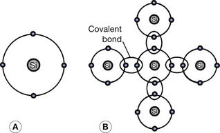
Figure 15.2 Pure silicon as an example of an intrinsic semiconductor. (A) A silicon atom showing the four electrons in its valence shell; (B) the covalent bonds formed in a pure silicon crystal by each silicon atom sharing electrons with four neighbouring silicon atoms.
Intrinsic semiconductors, which we just considered, have very limited practical use, due to their low conductivity. If small amounts of specific impurities are added to them (by a process called doping), they are then known as extrinsic semiconductors and have properties which allow us to use them as rectifiers and integrated circuits (ICs), all of which are found in most X-ray generators. Extrinsic semiconductors will now be discussed.
15.4 Extrinsic semiconductors
The addition of small amounts of specific impurities to silicon or germanium is the basis on which most extrinsic semiconductors are produced. The doping may be heavy or light, depending on the component being produced. A typical concentration is one part of impurity to 10 million parts of pure silicon. The electrical conductivity of the extrinsic semiconductor is much greater than that of an intrinsic semiconductor and the level of conductivity can be controlled by altering the ratio of doping material to pure material. The impurity atoms within the silicon crystal lattice are the source of this greatly increased electrical conductivity. This is because the type of impurity is chosen either to enhance electron flow in the conduction band (this gives an N-type semiconductor) or to enhance the flow of positive holes in the valence band (a P-type semiconductor). These two types of extrinsic semiconductor will now be considered.
15.4.1 N-type semiconductors
As we have seen, single atoms of intrinsic semiconductors have four valence electrons. To produce an N-type extrinsic semiconductor, a pentavalent impurity (one with five valence electrons) is used as the doping material. Arsenic, antimony and phosphorus are examples of pentavalent elements that are suitable. Figure 15.3 (See page 96) illustrates the effect of introducing an atom of phosphorus into the crystalline structure of silicon. Four of the valence electrons in the phosphorus form covalent bonds and the fifth electron is unbonded. This electron has an energy level which is just below the bottom of the conduction band (see Fig. 15.3B). At normal room temperatures, it is therefore virtually a free electron since it is easily lifted into the conduction band and can take part in electrical conduction if a potential difference is applied across the crystal.
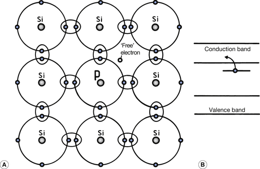
Figure 15.3 An example of an N-type extrinsic semiconductor. (A) The introduction of a pentavalent impurity produces a ‘free’ electron which does not take part in the covalent bond formation; (B) the energy of such free electrons is close to the conduction band so that they can readily be enabled to take part in electrical conduction.
Since such pentavalent atoms provide a ‘spare’ electron, they are known as donor impurities. It must be remembered that some electrons from the valence band will also be able to jump into the conduction band due to the normal vibrational energy within the atom at room temperature (this is similar to the intrinsic semiconductor; see Sect. 15.3). Positive holes will also be produced in the valence band and add to the conductivity. At normal room temperatures, this effect is much less than the effect produced by the donor atoms. In the case of an N-type semiconductor, the majority carriers are the electrons in the conduction band and the minority carriers are the holes in the valence band.
15.4.2 P-type semiconductors
As discussed in the previous section, the N-type semiconductor has enhanced conductivity because of the movement of electrons (negative, hence the N) so it is logical to assume that the P-type semiconductor functions because of the movement of positive holes. In the case of intrinsic semiconductors, we saw that holes were in the valence band, and that this allowed the movement of electrons within this band, giving the appearance of positive-hole movement (see previous Insight). In the P-type semiconductor, the movement of electrons within the valence band is encouraged by the creation of more positive holes within this band.
Figure 15.4 illustrates the result of introducing a trivalent material (one with three valence electrons) into a silicon crystal lattice. The material used in this case is aluminium, and it results in a broken covalent bond between it and the silicon atoms as there are not sufficient electrons in its outer shell to form the four covalent bonds. The energy level of this broken bond is only just above the valence band (Fig. 15.4B) and so, at normal room temperatures, electrons have sufficient energy to leap this small gap. Thus, the electrons, which have left the valence band of the silicon, leave positive holes behind them and so there is an increase in the number of positive holes in the valence band because of the trivalent impurity. This type of impurity is known as an acceptor impurity since it accepts electrons from the silicon atoms, creating holes in the valence band.
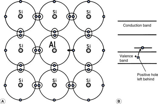
Figure 15.4 An example of a P-type extrinsic semiconductor. (A) The addition of a trivalent impurity produces a ‘hole’ in the outside electron shell; (B) such acceptor atoms take an electron from the valence band, leaving a positive hole capable of flowing through this band.
The majority carriers in the P-type material are positive holes in the valence band and the minority carriers are electrons that have sufficient energy to rise to the conduction band at room temperature, as in pure silicon (see Sect. 15.3.2).
Table 15.1 summarizes the main points we have considered so far regarding intrinsic semiconductors and the N-type and P-type of extrinsic semiconductor. Note that an increase in temperature does not affect the conductivity due to the majority carriers, but only that due to minority carriers. This is due to the increased numbers of electrons able to reach the conduction band from the valence band as the temperature increases.
Table 15.1 Summary of the properties of semiconductors
| INTRINSIC SEMICONDUCTOR | EXTRINSIC SEMICONDUCTOR | ||
|---|---|---|---|
| Typical material | Pure silicon or germanium | Silicon or germanium with added impurities | |
| Type of impurity | None | Pentavalent | Trivalent |
| Term for impurity | – | Donor | Acceptor |
| Conductivity | Low | High | High |
| Majority carrier | Electrons and positive holes in equal numbers | Electrons in conduction band | Positive holes in valence band |
| Minority carrier | – | Positive holes in valence band | Electrons in conduction band |
| Effect of temperature | Increases both the number of electrons and the number of positive holes | Increases number of minority carriers (positive holes) only | Increases number of minority carriers (electrons) only |
15.4.3 Diagrammatic representation of N- and P-types
When we discuss the PN junction in the next section, we need to form a mental picture of what occurs when an N-type and a P-type semiconductor are fused together. This is made easier if we have a simple symbolic representation of each, as shown in Figure 15.5. In the N-type, the majority carriers are the free donor electrons, represented by the minus (−) sign. Each nucleus of the donor impurity has an excess positive charge because of the loss of its outer electron. These fixed positive charges are represented by the circles enclosing the + sign. In the P-type, the positive holes are free and so are shown as a plus (+) sign while the electrons captured by acceptor atoms give these an overall negative charge. Since these atoms form part of the crystal lattice, they are not free to move so the minus sign is shown enclosed in the circles. Thus, in both the diagrams the ringed charges are fixed and the unringed charges are free or mobile.
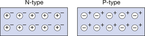
Figure 15.5 A diagrammatic representation of N- and P-type semiconductors. In both illustrations the ringed charges represent the fixed charges while the unringed charges represent the free charges which form the majority carriers (electrons for the N-type and positive holes for the P-type).
Note that in both the diagrams there are minority carriers caused by the elevation of electrons from the valence band to the conduction band. Since these play little part in the electrical properties of the material, they have been omitted from the diagrams for simplicity.
Before considering the PN junction in the following section in which the PN junction is discussed as a rectifier, let us first remember that the term diode applies to any two-electrode electrical device. The X-ray tube is an example of a thermionic diode as it has two electrodes – an anode and a cathode. Other examples of solid-state diodes used in radiography are light-emitting diodes (LEDs), which have replaced bulbs as indicators. LEDs operate in a forward-bias mode (see Sect. 15.5.2), while the photodiode is a semiconductor diode which converts light into electrical current in a reverse-bias mode (see Sect. 15.5.3), and has replaced the photo-multiplier valve in many applications where its smaller size, low power consumption and high current output are important, e.g. computed tomography (CT) scanners.
15.5 The PN junction
When P- and N-types are heat-fused together to form PN junctions, interesting effects appear. Examples of the PN junction include the junction diode, the transistor and the thyristor, which have one, two and three PN junctions respectively.
If we use the diagrammatic representation that we have just discussed, then the PN junction may be shown as in Figure 15.6. When P- and N-types are brought together and heat-fused in intimate contact, free electrons from the N-type and free positive holes from the P-type are able to penetrate across the boundary between them. This diffusion of charge across the barrier results in recombination of the positive holes and the free electrons (the free electrons drop into the positive holes so that their charges are cancelled; see Sect. 15.3.1). Thus, for a short distance on either side of the PN junction (about 0.5×10⁻⁶ m), no free carriers exist – this is known as a depletion layer. However, a net charge exists on either side of the junction because the N-type has lost electrons and the P-type has lost positive holes (Fig. 15.6B), resulting in a negatively charged area just within the P-type region and a positively charged area just within the N-type region. The two peaks of charge shown in Figure 15.6 increase in size until no further net flow of majority carriers takes place. For example, a free electron from the N-type will only be able to pass over to the P-type if it has sufficient energy to overcome the repulsion of the negative peak at the PN junction.
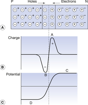
Figure 15.6 The PN junction. (A) The diffusion of electrons across the PN junction in one direction and positive holes in the other forms a charge barrier, which prevents further flow. (B) Gain in charge across the junction and (C) potential difference established across the barrier.
The charge distribution produces its own potential difference, as depicted in Figure 15.6C. The height of CD is known as the potential barrier since it acts in opposition to the flow of majority carriers from either side of the barrier. For a silicon PN junction, this potential barrier is about 0.4 eV, so free carriers of energy lower than 0.4 eV cannot overcome this barrier.
15.5.1 Minority carriers at the PN junction
The above discussion concerned only the effect of the PN junction on the majority carriers. For majority carriers, a potential barrier is formed which prevents any further flow. However, this barrier actually aids the transport of minority carriers between the materials. Consider the potential gradient between D and C (Fig. 15.6). If a free electron (the minority carrier in a P-type material) is in position D, it is strongly attracted by the positive potential of the N-type material and rapidly moves to C. At equilibrium, of course, there are equal numbers of minority carriers moving in both directions.
Minority carriers are dependent on temperature, since an increase in temperature increases the number of electrons which can jump from the valence to the conduction band. Thus, the flow of minority carriers across a PN junction increases with temperature. This affects the behaviour of the PN junction under conditions of reverse bias, as will be explained later in this chapter.
15.5.2 Forward bias
If a source of potential difference (e.g. a battery) is connected across a PN junction, as shown in Figure 15.7A, then a current will flow across the junction because the potential barrier is lowered. This is shown graphically in Figure 15.7B (See page 48). The negative side of the battery reduces the positive potential of the N-type and the positive side of the battery reduces the negative potential of the P-type. The original height of the barrier is lowered and energetic free carriers from either side are able to surmount the barrier. A steady electrical current is set up as long as the battery is connected. This type of connection, which produces current flow across the PN junction, is called forward bias. The removal of the battery results in the full height of the barrier being re-established and so no further current can flow.
15.5.3 Reverse bias
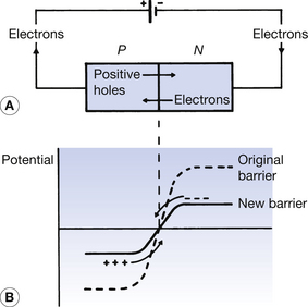
If the source of potential difference is now connected in the opposite orientation, as shown in Figure 15.8A, then this is known as reverse bias. No current flows through this circuit due to the increase in the potential barrier at the PN junction. The graph in Figure 15.8B shows that the negative side of the battery increases the negative potential of the P-type and the positive side of the battery increases the positive potential of the N-type. Thus, no current flows, as none of the majority carriers has sufficient energy to surmount this higher barrier. In fact, when a PN junction is connected in reverse bias, the depletion layer extends further into each semiconductor on either side of the PN junction.
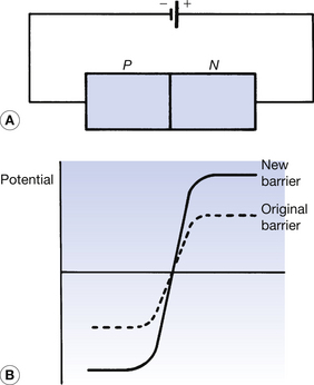
Figure 15.8 (A) The PN junction connected in reverse bias. The potential from the battery raises the potential barrier, as shown in (B), and further prevents electrical conduction.
The discussion so far has been regarding majority carriers. However, as discussed earlier, a small electrical current due to the thermally generated minority carriers is able to flow.
The PN junction can act as a one-way valve (a diode) which allows current only to flow in one direction. For this reason, PN junctions are used to create solid-state rectifiers or PN junction diodes. The symbol for such a device is shown below.
15.5.4 The PN junction as a diode
In our discussion in the last two sections we have shown that current will readily flow through a PN junction when it is forward biased, but very little current will flow through the junction when it is reverse biased. Thus, the PN junction can act as a one-way valve (a diode) allowing current to flow in only one direction. For this reason, PN junctions are used to create solid-state rectifiers or PN junction diodes. The symbol for such a device is:
Note that electrons may only flow through the diode against the direction of the arrow or bar of the symbol. Such devices have replaced thermionic diodes for the following reasons:
• They contain no filament and thus have a longer life, consume less power and produce less heat.
• They are smaller in size than thermionic diodes, thus enabling the production of a more compact X-ray unit.
• They have a smaller forward voltage drop than thermionic rectifiers and are more efficient rectifiers enabling a higher kVp to be applied to the X-ray tube (see Ch. 30).
15.5.5 PN Junction characteristics
If the current flowing through a PN junction is plotted against the potential difference across it, then the graph produced is referred to as the characteristic curve for the device. Such a graph is shown in Figure 15.9. As the potential difference across the diode is increased in a forward direction, so the current through it increases, as shown by OA on the figure. If we compare this with the forward-bias characteristic for the vacuum diode, we can note that, in this case, there is no saturation current. However, passing too high a current through a PN junction diode can cause irreparable damage.
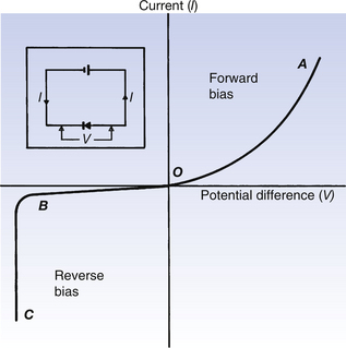
A normal reverse bias produces only a very low reverse current due to the flow of minority carriers that happen to move into the vicinity of the PN junction and so get swept across it. As already discussed, this reverse current is very sensitive to temperature as this alters the production of minority carriers due to thermal excitation. If the reverse bias is further increased, then the reverse current increases dramatically (see BC in Figure 15.9 (See page 100)). This is called the zener voltage or breakdown voltage and at this value of reverse bias the diode ceases to act effectively as a rectifier. At this negative bias, the minority carriers that cross the potential barrier gain enough energy to ionize atoms with which they collide. This results in the liberation of additional electrons and hence the large current. This phenomenon is also referred to as solid-state multiplication or electron avalanching.
A zener diode is a type of diode that permits current not only in the forward direction like a normal diode, but also in the reverse direction if the voltage across it is larger than the breakdown voltage. This is known as zener knee voltage or zener voltage. The zenner diode acts as a protective device by limiting the output voltage to components on its output side while the zenner voltage is passedto earth.
15.6 Integrated circuits
This section gives an overview of the history and production of a ‘typical’ integrated circuit (IC). The concept of the IC was proposed by Godffrey Dummer of the Royal Radar Establishment of the British Ministry of Defenses in 1952, although the first working ICs were not produced until 1959 by two Americans. By current standards these circuits were very crude as they contained many discrete components such as miniaturized transistors, resistors and capacitors. By the early 1960s, extensive use of semiconductors had replaced many circuits which had previously used thermionic valves.
As technology improved, the number of components on ICs or ‘chips’ increased leading to dedicated chips such as counters, adders and amplifier chips. ICs of this type are still available and used in some applications today.
15.6.1 The development of ICs
Table 15.2 gives a brief outline of the development of the integrated circuit. For more details, the reader is advised to consult specialized texts on integrated circuits.
Table 15.2 The development of the integrated circuit
| YEAR PRODUCED | ABBREVIATION | NAME/FEATURES | NUMBER OF TRANSISTORS IN CIRCUIT |
|---|---|---|---|
| Early 1960s | SSI | Small scale integration | Tens |
| Late 1960s | MSI | Medium scale integration | Hundreds |
| Resistors, capacitors and inductances added to wafer as part of etching stages | |||
| 1970s | LSI | large scale integration | Tens of thousands |
| 1980s | VLSI | Very large scale integration | Hundreds of thousands |
| Possible to produce microprocessors (CPUs) | |||
| Early 1990s | ULSI | Ultra large scale integration | More than a million |
| Increased CPU speeds | |||
| Late 1990s | ULSI | Ultra large scale integration dual core processors | Hundreds of millions |
| Increased CPU speeds |
15.6.2 The manufacturing process
Hundreds of ICs are made at the same time on a single, thin slice of silicon and are then cut apart into individual IC chips. The manufacturing process takes place in a tightly controlled environment known as a clean room. Since some IC components are sensitive to certain frequencies of light, even the light sources are filtered.
Manufacturing processes vary depending on the integrated circuit being made. The following process is typical. The process commences with a chemically pure cylindrical ingot of silicon about 100 mm in diameter, and then thin, round wafers of silicon are cut off the ingot by a wafer slicer. Each wafer is about 0.1 mm thick. The surface on which the integrated circuits are to be formed is polished. The surfaces of the wafer are then coated with a layer of silicon dioxide to form an insulating base and to prevent any oxidation of the silicon which would cause impurities.
15.6.2.1 Masking
The complex and interconnected design of the circuit components is prepared in a process similar to that used to make printed circuit boards. For ICs, however, the dimensions are much smaller and there are many layers superimposed on top of each other. These layers can contain components such as resistors, capacitors and inductances. The design of each layer is prepared on a computer-aided drafting machine, and the image is made into a mask which will be optically reduced and transferred to the surface of the wafer. Each layer has its own mask which is opaque in certain areas and clear in others. It has the images for all of the several hundred integrated circuits to be formed on the wafer.
The wafer is first coated with a layer of photo-resist and is then baked to remove the solvent. It is then irradiated with light. Because the spaces between circuits and components are so small, ultraviolet light, which has a very short wavelength, is used as it can pass through the tiny clear areas on the mask. Beams of electrons or X-rays are also sometimes used to irradiate the photo-resist. The layer is the subjected to chemical etching which ‘opens’ the clear areas of the mask and the first doping process is carried out to create a layer of P- or N-regions.
15.6.2.2 Doping
Two methods of doping may be used:
1. Atomic diffusion is a method of adding dopants to create a layer of P- or N-regions. In this method, a batch of wafers is placed in a quartz tube oven surrounded by a heating element. Here the wafer is exposed to a temperature between 1816 and 1205°C; the dopant chemical is then carried in on an inert gas. As the gas passes over the wafers, the dopant is deposited on the hot surfaces left exposed by the masking process. This method is suited to doping relatively large areas, but is not accurate for smaller areas. There are also some problems with the repeated use of high temperatures as successive layers are added.
2. The second method to add dopants is ion implantation. In this method, a dopant gas, such as phosphune or boron trichloride, is ionized to provide a beam of high-energy dopant ions which are fired at specific regions of the wafer. These ions penetrate the wafer and remain implanted. The depth of penetration can be controlled by altering the beam energy, and the amount of dopant can be controlled by altering the beam current and time of exposure. Schematically, the whole process resembles firing a beam in a bent cathode ray tube. This method is so precise that it does not require masking – just point and shoot the dopant where it is needed. However, it is much slower than the atomic diffusion process.
15.6.3 Making successive layers
The existing layer of photo-resist is removed, and another layer of photo-resist is added for the next layer. The process of etching or doping is repeated. Sometimes a layer of silicon dioxide is laid down to provide an insulator between layers or components. The etching and doping process continues for each successive layer until all of the layers are completed. A final silicon dioxide layer seals the surface, and final etching opens up contact points, when a layer of aluminum is deposited to make the contact pads. At this point, the individual ICs are tested for electrical function and any chips failing the test are identified.
15.6.4 Making individual ICs
The thin wafer is like a piece of glass. The hundreds of individual chips are separated by scoring a cross-hatch of lines with a fine diamond cutter on the wafer and then putting it under stress to cause each chip to separate. Those ICs that fail the electrical test are discarded. Further inspection under a microscope reveals chips damaged by the separation process; all faulty chips are then discarded.
The good ICs are individually bonded into their mounting package and the thin wire leads are connected by either ultrasonic bonding or thermocompression. The mounting package is marked with identifying part numbers and other information.
Finally the completed ICs are sealed in antistatic plastic bags to be stored or shipped to the end user.
15.6.5 Hazardous materials and recycling
The dopant substances used – gallium and arsenic among others – are toxic, and their storage, use and disposal must be tightly controlled.
Because IC chips are so versatile, a significant recycling industry has sprung up. Many ICs and other electronic components are removed from otherwise obsolete equipment, tested and resold for use in other devices.
15.6.6 The future
It is difficult to tell with any certainty what the future of the IC is. Changes in technology since the device’s invention have been rapid, but evolutionary. Many changes have been made in the architecture, or circuit layout, on a chip, but the IC still remains a silicon-based design.
The next major leap in the advancement of electronic devices (if such a leap is to come) may involve an entirely new circuit technology. Better devices than the very best microprocessor have always been known to be possible. The human brain, for example, processes information much more efficiently than any computer, and some futurists have speculated that the next generation of processor circuits will be biological rather than mineral. At this point in time, such matters are the stuff of fiction. There are no immediate signs that the IC is in any danger of extinction.
15.7 Semiconductor devices in radiography
Semiconductor devices are used extensively in radiography. This chapter has given a brief overview of some of the types that are used. The development of ICs in the 1960s resulted in the production of complete miniaturized circuits which now perform many of the functions previously carried out by discrete solid-state or by ICs. ICs are produced on a single chip of silicon about 1 mm square and about 0.1 mm thick. This process, using ULSI, is able to produce circuits containing in excess of over 100 million transistors per chip. This technology offers components of very high reliability at very low production costs. There is also significant space saving over electromechanical devices. Both of the above have resulted in many of the circuits in modern X-ray generators containing significant amounts of ‘chip technology’.
The microprocessor is another development based on silicon chip and ULSI technology. Using Boolean logic and inbuilt programs, microprocessors are used to monitor and control many pieces of equipment used in radiography.
The full description of the function of such ICs is the subject of a book in its own right and as such is beyond the short introduction in this text.
Table 15.3 outlines some of the applications of semiconductor technology in radiography
Table 15.3 Applications of semiconductor devices
| SEMICONDUCTOR DEVICE | APPLICATIONS |
|---|---|
| Solid-state diode | Rectification of the high-tension supply to the X-ray tube using multiple PN junctions connected in series to form stick rectifiers Rectification of the supply to devices that require a unidirectional supply, e.g. solid-state ‘chips’ |
| Transistors | Electronic timing circuits |
| Safety interlocks that avoid exceeding the rating of the X-ray tube | |
| Triacs | Primary switching of the X-ray exposure, i.e. the triac switches the exposure on and off – following the signal from the timer |
| Integrated circuits (ICs) | ICs have replaced many semiconductor devices, with the exception of HT diodes These can check that a number of functions have taken place in sequence, e.g. they can check that the anode is rotating at the correct speed before an exposure is made |
| Microprocessors | These have many applications in more sophisticated measurement and controls, e.g. microprocessors can check a certain set of exposure factors to ensure that they are not outside the rating of the selected tube focus |
In this chapter, you should have learnt the following:
• A semiconductor has a conductivity between that of an insulator and a conductor, reflecting the small energy gap between the conduction and the valence bands (see Sect. 15.3).
• An intrinsic semiconductor, such as silicon, is a chemically pure semiconductor with a regular arrangement of atoms within its crystal lattice (see Sects 15.3 and 15.3.2).
• Extrinsic semiconductors have carefully measured quantities of impurity added to the intrinsic semiconductor by a process known as doping (see Sect. 15.4).
• An N-type semiconductor is produced when a pentavalent or donor impurity is added to the silicon. This gives a supply of free electrons in the semiconductor (see Sect. 15.4.1).
• A P-type semiconductor is produced when a trivalent or acceptor impurity is added to the silicon. This gives a supply of positive holes within the semiconductor (see Sect. 15.4.2).
• The majority carrier in the N-type material is the free electron and the majority carrier in the P-type is the free positive hole (see Sects 15.4.1 and 15.4.2).
• Minority carriers are thermally produced and are present in all types of semiconductor at room temperature. Minority carriers in the N-type are positive holes and in the P-type are free electrons (see Sects 15.4.1 and 15.4.2).
• A PN junction produces a potential barrier to the flow of electrons and holes. The height of this barrier grows when the junction is reverse biased and diminishes when the junction is forward biased. Thus the PN junction will allow current to flow in one direction only – electrons can flow from N to P (see Sect. 15.5).
• The development and production of integrated circuits (see Sect. 15.6).
• Some of the applications of semiconductor devices in radiography (see Sect. 15.7).